

About Us
This laboratory was established in April 2002 as the next-generation computing research subdivision of the Electrical Communication Laboratory Brain Computing Research Division. In the reorganization of 2004, it became a member of the Brainware Experiment Facility and the name was changed to the Brain Architecture Research Department. As of 2008, it became the New Paradigm VLSI System Laboratory.
 |
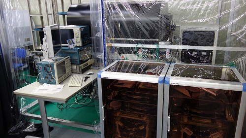 |
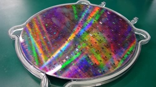
In this laboratory, we focus on the research of very large scale integrated-circuit (VLSI) design technology. Traditionally, increased performance and reliability of VLSI systems has been acomplished through incremental refinement of material and device manufacturing. However, performance improvement due to this miniaturization technology is expected to soon reach its limit. We aim to surpass the limits of conventional VLSI systems through new paradigm system architectures that actively exploit new materials and device characteristics alongside conventional CMOS design. Multi-value current-mode integrated circuits and asynchronous network-on-a chip (NoC) architectures attempt to solve the problem of wiring in next-generation VLSI, while logic-in-memory computing achieves huge memory bandwidth by dispersing storage throughout arithmetic circuits using nonvolatile ferroelectric, magnetic tunnel junction (MTJ), and phase-change memory devices.
A VLSI chip that functions as the brain of electronic equipment and the VLSI system to which it is applied are important technologies that form the basis of industrial products and infrastructure in modern society. In this laboratory, we aim to realize a powerful and multipurpose VLSI chip that not only mimics the processing capability, but also intellectual activity of the human brain, while seeking out new design paradigms through the fusion of device, circuit, and architecture technology. We hope to develop various fields of research while collaborating with researchers both in Japan and abroad.